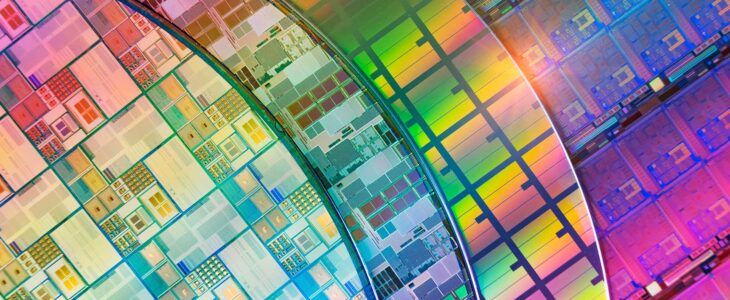
The relentless pursuit of miniaturization and performance in the semiconductor industry has pushed the boundaries of what’s possible. Smaller transistors deliver faster processing speeds, but they also introduce new challenges, particularly when it comes to reliability. Burn-in, a crucial process for identifying and weeding out potential early life failures (ELFs) in integrated circuits (ICs), becomes even more critical as power densities and operating temperatures rise.
Traditionally, burn-in has been performed at the package level, after individual die are singulated (separated) from the wafer and housed in packages. However, with increasing power densities, traditional package-level burn-in approaches are reaching their limits. This has led to the rise of wafer-level burn-in (WLBI), a powerful technique that offers significant advantages for ensuring the reliability of high-performance ICs.
This article delves into the world of wafer-level burn-in, exploring its benefits, challenges, and the role KES Systems plays in providing cutting-edge solutions for high-power applications. We’ll leverage insights from industry resources, including relevant articles and KES Systems’ expertise (kessystemsinc.com), to paint a comprehensive picture of this transformative technology.
The Need for Burn-In: Identifying Weaknesses Before Deployment
Imagine a brand-new smartphone: sleek, powerful, and packed with the latest technology. Yet, within its intricate circuitry, there might lurk a hidden weakness – a microscopic flaw that could lead to premature device failure. This is precisely where burn-in comes in.
Burn-in is a stress test designed to accelerate the aging process of an IC. By subjecting the device to elevated temperatures, voltages, and currents beyond its normal operating conditions, engineers can uncover latent defects that might otherwise go unnoticed during standard functional testing. Early detection allows for the removal of faulty devices, preventing costly field failures and ensuring the long-term reliability and performance of the final product.
The Importance of Burn-in in Today’s Semiconductor Landscape:
- Smaller, Denser Devices: As transistor sizes shrink and chip densities increase, the risk of early life failures also grows. Leakage currents and thermal management become more critical, necessitating thorough burn-in procedures.
- High-Performance Applications: With the rise of artificial intelligence (AI), 5G communication, and high-performance computing (HPC), ICs are operating at ever-increasing power levels. Traditional package-level burn-in struggles to effectively stress these high-power devices.
- Improved Quality and Yield: By catching defects early through burn-in, manufacturers can significantly improve overall yield and product quality. This translates to cost savings and a more reliable end product.
The Package-Level Burn-In Bottleneck: Limitations and Challenges
For decades, the semiconductor industry has relied on package-level burn-in as the primary method for identifying early life failures. In this approach, individual die are singulated from the wafer, housed in individual packages, and then subjected to electrical stress at elevated temperatures.
Challenges with Package-Level Burn-In:
- Heat Dissipation: As power densities rise, the ability of packages to dissipate the heat generated during burn-in becomes a limiting factor. This restricts the effectiveness of stress testing high-power devices.
- Increased Costs: Package-level burn-in requires additional handling and processing steps, adding to the overall cost of production.
- Lower Efficiency: Testing individual packaged devices can be a time-consuming and resource-intensive process, impacting production throughput.
The Rise of Wafer-Level Burn-In: A New Era of Reliability Testing
Wafer-level burn-in (WLBI) emerges as a transformative solution, addressing the limitations of package-level burn-in and paving the way for a more efficient and effective approach. In WLBI, the burn-in process is conducted while the die are still on the wafer, before being singulated and packaged.
Benefits of Wafer-Level Burn-In:
- Superior Power Handling: WLBI systems can handle higher power levels compared to package-level testers, enabling effective stress testing of high-power devices.
- Improved Efficiency: Testing all die on the wafer simultaneously leads to significantly faster throughput and improved production efficiency.
- Cost Reduction: Eliminating individual package handling and testing reduces overall production costs.
- Earlier Defect Detection: WLBI allows for the identification of defects at an earlier stage in the fabrication process, facilitating corrective actions and improving overall yield.
While WLBI offers numerous advantages, certain challenges remain. Ensuring reliable electrical contact with all die on the wafer and managing the significant heat generated during burn-in are key considerations.
KES Systems: Leading the Way in High-Power Wafer-Level Burn-In Solutions